用户:Schenad/气态探测器
气体式探测器(英语:gaseous detection device,GDD)泛指在环境电子显微镜或类似的扫描式设备中能够在一定的气压下对电子信号进行测量的仪器。
传统的电子探测器(例如埃弗哈特-索恩利探测器)需在较高的真空(低于10-3Pa或10-5Torr)才能工作。气体式探测器应用了不同的原理探测电子,工作环境可以覆盖到较低的真空(50Pa或0.38Torr[1])。气体式探测器的出现使得通过电子显微镜技术观测一些在真空下无法维持其自然形态的样品(例如生物组织、胶体和某些液体等)成为可能。如今,占有电子显微镜市场上超过50%的份额的可变压电子显微镜(VP-SEM)或环境电子显微镜(ESEM)的系统内都可以见到气体式探测器的应用。[2]
历史
[编辑]传统扫描电子显微镜内部的电子探测器需要在真空下才能工作;这大大限制了其可观测的样品。为了对真空下无法维持自身原本形态的样品(例如生物组织、胶体和某些液体等)进行观测,一类被称作“环境电子显微镜”的新型电子显微镜应运而生。这一类电子显微镜能够在低真空,甚至是在一个大气压的环境下对样品进行观测。搭载在环境电子显微镜上的电子探测器继承了传统扫描电子显微镜使用的一部分电子探测器并进行了一定的改造,使其在低真空下也能工作。例如,通过设计合适的几何位置来优化电子束传输、背散射电子分布和光波导传输可以改进背散射电子探测器[3]。然而,传统扫描电子显微镜常用的二次电子探测器(或埃弗哈特-索恩利探测器)上采用了高电势的设计;即使在低真空的条件下,该探测器也会出现灾难性的击穿,因此无法简单地直接改造。1983年,Danilatos[4]设计了基于完全不同原理的探测器,解决了这一难题。借助不同信号对气体的电离作用,环境中的气体被当作了探测器的一部分。若对电极的配置和偏压进行合适的控制,即可实现对二次电子的探测。气体式探测器工作原理的已被发表为一篇综述[5];下述的大部分内容都来源于此篇综述。
原理
[编辑]
气体式探测器由核物理和天文学中对粒子的观测手段改造而来。成像所需的参数需要考虑样品腔(specimen chamber)的电子显微镜,以及腔内气体存在时的情况。虽然由电子束-样品相互作用产生的信号与周围气体会发生气态电离和激发,但是信号-气体相互作用的类型、强度和分布各不相同。幸运的是,这些相互作用通常能够兼容环境电子显微镜成像所需的恒定时间(time-constant)的要求。确立这种兼容性促成了气体式探测器的发明以及从粒子物理学到电子显微镜领域实现跨越的基础。参与信号-气体相互作用的主要包括背散射电子和二次电子。
实现方式
[编辑]

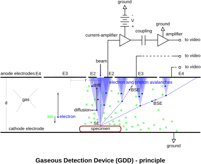
右图所展示的气体式探测器原理不仅有二次电子模式,还包括了背散射电子模式以及二者的组合。即使只想单独使用SE信号,也建议至少再使用一个同心电极来帮助分离BSE干扰以及其他噪音源,比如气体散射出的裙边电子。这个附加部分可以作为“守护”电极,并且通过独立调节其偏置与SE电极相比,可以有目的地控制图像对比度。还可使用其他控制电极,例如阳极和阴极之间的网格。 Even if only the SE signal is desirable to use alone, at least one additional concentric electrode is recommended to employ in order to help in the separation from interference of BSE and also from other noise sources such as the skirt electrons scattered out of the primary beam by the gas. This addition may act as a “guard” electrode, and by varying its bias independently from the SE electrode, the image contrast can be controlled purposefully. Alternative control electrodes are used such as a mesh between anode and cathode.[5] A multipurpose array of electrodes below and above the specimen and above the pressure limiting aperture of the ESEM has also been described elsewhere.[6]
The development of this detector has required devoted electronics circuitry, especially when the signal is picked up by the anode at high bias, because the floating current amplified must be coupled at full bandwidth to the ground amplifier and video display circuits (developed by ElectroScan).[6] An alternative is to bias the cathode with a negative potential and pickup the signal from the anode at floating ground without the need for coupling between amplifier stages. However, this would require extra precaution to protect users from exposure to a high potential at the specimen stage.
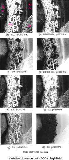
A further alternative that has been implemented at the laboratory stage is by the application of a high bias at the anode but by pickup of the signals from the cathode at floating ground, as shown in the accompanying diagram.[7] Concentric electrodes (E2, E3, E4) are made on a copper-coated fiberglass printed circuit board (PCB) and a copper wire (E1) is added at the center of the disk. The anode is made again from the same PCB with a conical hole (400 micrometres) to act as a pressure limiting aperture in the ESEM. The exposed fiberglass material inside the aperture cone together with its surface above are coated with silver paint in continuity with the copper material of the anode electrode (E0), which is held at high potential. The cathode electrodes are independently connected to ground amplifiers, which, in fact, can be biased with low voltage directly from the amplifier power supplies in the range of ±15 volts without any further coupling required. On account of the induction mechanism operating behind the GDD, this configuration is equivalent to the previous diagram, except for the inverted signal that is electronically restored. While electrode E0 is held at 250 V, meaningful imaging is done as shown by a series of images with composition of signals from various electrodes at two pressures of supplied air. All images show part of the central copper wire (E1), exposed fiber-glass (FG, middle), and copper (part of E2) with some silver paint used to attach the wire. The close resemblance of (a) with (b) at low pressure and (c) with (d) at high pressure is a manifestation of the principle of equivalence by induction. The purest SE image is (e) and the purest BSE is (h). Image (f) has prevailing SE characteristics, whilst (g) has a comparable contribution of both SE and BSE. Images (a) and (b) are dominated by SE with some BSE contribution, whilst (c) and (d) have comparable contribution by both SE and BSE.
The very bright areas on the FG material result from genuine high specimen signal yield and not from erratic charging or other artifacts familiar with plastics in vacuum SEM. High yield of edges, oblique incidence, etc. can for the first time be studied from the true surfaces without obstruction in ESEM. Mild charging, if present, may produce stable contrast characteristic of material properties and can be used as a means for studies of the physics of the surfaces.[7] The images presented in this series are reproductions from photographic paper with limited bandwidth, on which attempting to bring up detail in dark areas results in saturating the bright areas and vice versa, whilst a lot more information is usually contained on the negative film. Electronic manipulation of the signal together with modern computer graphics can overcome some old imaging limitations.
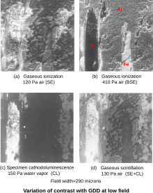
An example of the GDD operating at low voltage is shown with four images of the same field of view of a polished mineral containing aluminum, iron, silicon and some unknown surface impurities. The anode electrode is a single thin wire placed on the side and below the specimen surface, several mm away from it.[8] Image (a) shows predominantly SE contrast at low pressure, whilst (b) shows BSE material contrast at higher pressure. Image (c) shows cathodoluminescence (CL) from the specimen surface by use of water vapor (which does not scintillate), whilst (d) shows additional photon signal by changing the gas to air which scintillates by signal electrons originating from the specimen. The latter appears to be a mixture of CL with SE, but it may also contain additional information from the surface contaminant charging to a varying degree with gas pressure.
The GDD at high voltage has clear advantages over the low voltage mode, but the latter may be used easily with special applications such as at very high pressures where the BSE produce a high ionization gain from their own high energy, or in cases when the electric field requires shaping to purposeful ends. In general, the detector should be designed to operate at both high and low bias levels including variable negative (electron retarding) bias[9] with important contrast generation.
Further improvements have been envisaged, such as the use of special electrode materials, gas composition and shaping the trajectory of detection electrons by special electric and magnetic fields (page 91).[5]
商业化
[编辑]第一个成功商业化的气体式探测器来自于ElectroScan公司[10]。他们推出了首字母缩写为ESD的“environmental secondary detector”(环境二次电子探测器)。之后其改进版本——“gaseous secondary electron detector”(气体式二次电子探测器,GSED)也随之发布。在电子显微镜的物镜中使用磁场也可见于另一商业专利中[11]。LEO公司(现在的Carl Zeiss SMT[12])开发了其环境电镜气体式探测器的闪烁模式(scintillation mode)和电离模式(ionization mode),能够在低真空且较大范围的真空条件下工作。
参考资料
[编辑]- ^ Scanning electron microscopy and x-ray microanalysis 3rd. Kluwer Academic/Plenum Publishers. : 239. ISBN 9780306472923.
- ^ Scanning electron microscopy and x-ray microanalysis 3rd. Kluwer Academic/Plenum Publishers. : 220. ISBN 9780306472923.
- ^ Danilatos, G.D. Design and construction of an atmospheric or environmental SEM (part 3). Scanning. 1985, 7: 26–42. doi:10.1002/sca.4950070102.
- ^ Danilatos, G.D. A gaseous detector device for an environmental SEM. Micron and Microscopica Acta. 1983-01, 14 (4): 307–318. doi:10.1016/0047-7206(83)90002-X.
- ^ 5.0 5.1 5.2 Danilatos, G.D. Theory of the Gaseous Detector Device in the Environmental Scanning Electron Microscope. Advances in Electronics and Electron Physics (Elsevier). 1990: 1–102 [2018-11-09]. doi:10.1016/s0065-2539(08)60388-1.
- ^ 6.0 6.1 美国专利第4,897,545号, filed October 14, 1988 (priority date October 16, 1987, Australia PI4918). Assigned to ElectroScan Corp. Inventor: GD Danilatos
- ^ 7.0 7.1 Danilatos, G.D. Mechanisms of detection and imaging in the ESEM. J. Microsc. 1990, 160: 9–19. doi:10.1111/j.1365-2818.1990.tb03043.x.
- ^ Danilatos, G.D. Cathodoluminescence and gaseous scintillation in the environmental SEM. Scanning. 1986, 8: 279–284. doi:10.1002/sca.4950080605.
- ^ Danilatos, G.D. Equations of charge distribution in the ESEM. Scanning Microscopy. 1990, 4 (4): 799–823.
- ^ 美国专利第4,785,182号, filed May 21, 1987. Secondary electron detector for use in a gaseous atmosphere. Inventors: J.F. Mancuso, W.B. Maxwell, G.D. Danilatos. Assignee: ElectroScan Corporation.
- ^ 美国专利第6,972,412号, (December 6, 2005) Particle-optical device and detection means. Inventors: Scholtz Jacob Johannes, Knowles W. Ralph, Thiel Bradley Lamar, Van Veen Gerardus, Schroemges Rene Peter Marie
- ^ Carl Zeiss SMT ESEM
外部链接
[编辑][[Category:顯微鏡]] [[Category:显微术]] [[Category:科学技术]]
